When we use the cloud for heavy duty computations, we quickly find out that although storage is inexpensive, we never know how fast we can access our data. If we want guaranteed performance in terms of IOPS, the price quickly goes up. This has to do with the distance the data has to travel. In a warehouse-scale datacenter, we have two cabling lengths: up to a couple meters for vertical networking in a rack and up to a couple hundred meters for horizontal networking between racks. There are some game-changing technology developments on the horizon regarding the horizontal networking.
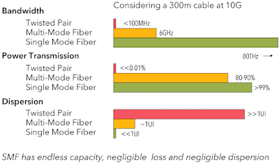
For the vertical cabling, copper can be used, but for the horizontal cabling fiber optics has to be used due to dispersion, as shown in the figure below.
Since the processor is electronic, at each end of the optical fiber cable we need an expensive transducer. Chip companies have invested substantial resources trying to grow lasers on CMOS chips to feed an optical cable, but the physical manufacturing process was very messy and never worked well.
The breakthrough came a dozen years ago with the development of nanotechnology to fabricate devices based on the optical bandgap. This allowed to take a PowerPC processor, make it flat, then use nanotechnology to grow an optical resonance ring on top of it. Now the laser source can be external to the chip and make a round in the ring while being modulated from the PowerPC. This was a seminal breakthrough.
At the end of July, Jürg Leuthold, professor of photonics and communications at ETH Zurich, and his colleagues had another seminal breakthrough. Hitherto, miniaturization of the modulator has been limited by the wavelength of the laser. In order to beat that limit and to make the device even smaller, the light is first turned into so-called surface plasmon polaritons (SPP). Plasmon polaritons are a combination of electromagnetic fields and electrons that propagate along a surface of a metal strip. At the end of the strip, they are converted back to light once again. The advantage of this detour is that plasmon polaritons can be confined in a much smaller space than the light they originated from. The signal is created by modulating the plasmon-polaritons in an interferometer.
By applying a voltage, the refractive index and hence the velocity of the plasmons in one arm of the interferometer can be varied, which in turn changes their amplitude of oscillation at the exit. After that, the plasmons are re-converted into light, which is fed into a fiber optic cable for further transmission.
This is the cheapest modulator ever built. It is very simple, consisting of a gold layer on glass that is only 150 nm thick and an organic material whose refractive index changes when an electric voltage is applied and that thus modulates the plasmons inside the interferometer. As such a modulator is much smaller than conventional devices and it consumes very little energy—only a few thousandth of Watts at a data transmission rate of 70 Gigabits per second. This corresponds to merely a hundredth of the consumption of commercial models.
Source: Nature Photonics 9, 525–528 (2015), doi:10.1038/nphoton.2015.127.
New technologies take a few years to evolve from universities to industrial research labs and then to industry. One of the accelerators of this process is CERN, in particular, the Large Hadron Collider (LHC) project. The detectors produce about 25 PB of data each year, which travel through more than 100,000 optical links to obtain the required bandwidth. The distance from the detectors to the control rooms is about 150 m and the connectors have to be able to withstand the 3.8 Tesla magnetic field in the detector and enormous levels of radiation.
For this application, scientists at CERN have developed so-called “versatile-link” optical components with a minimal energy consumption. By 2018 Marcel Zeiler and his colleagues will have new modulators—of course, also based on interferometry—that can withstand the harsh environment in the LCH.
Source: SPIE Professional October 2015.
Although in a datacenter the radiation is negligible and the magnetic fields are very far from Teslas, the experience is that CERN technology transitions to industry very fast, so we should not be surprised to see new generation versatile optical links in a year or two at most. The capability of economically moving data for hundreds of meters on 100 Gigabit Ethernet (100GbE) links renders old architectures like Hadoop moot because there is no reason for moving the data to HDFS for MapReduce.


No comments:
Post a Comment